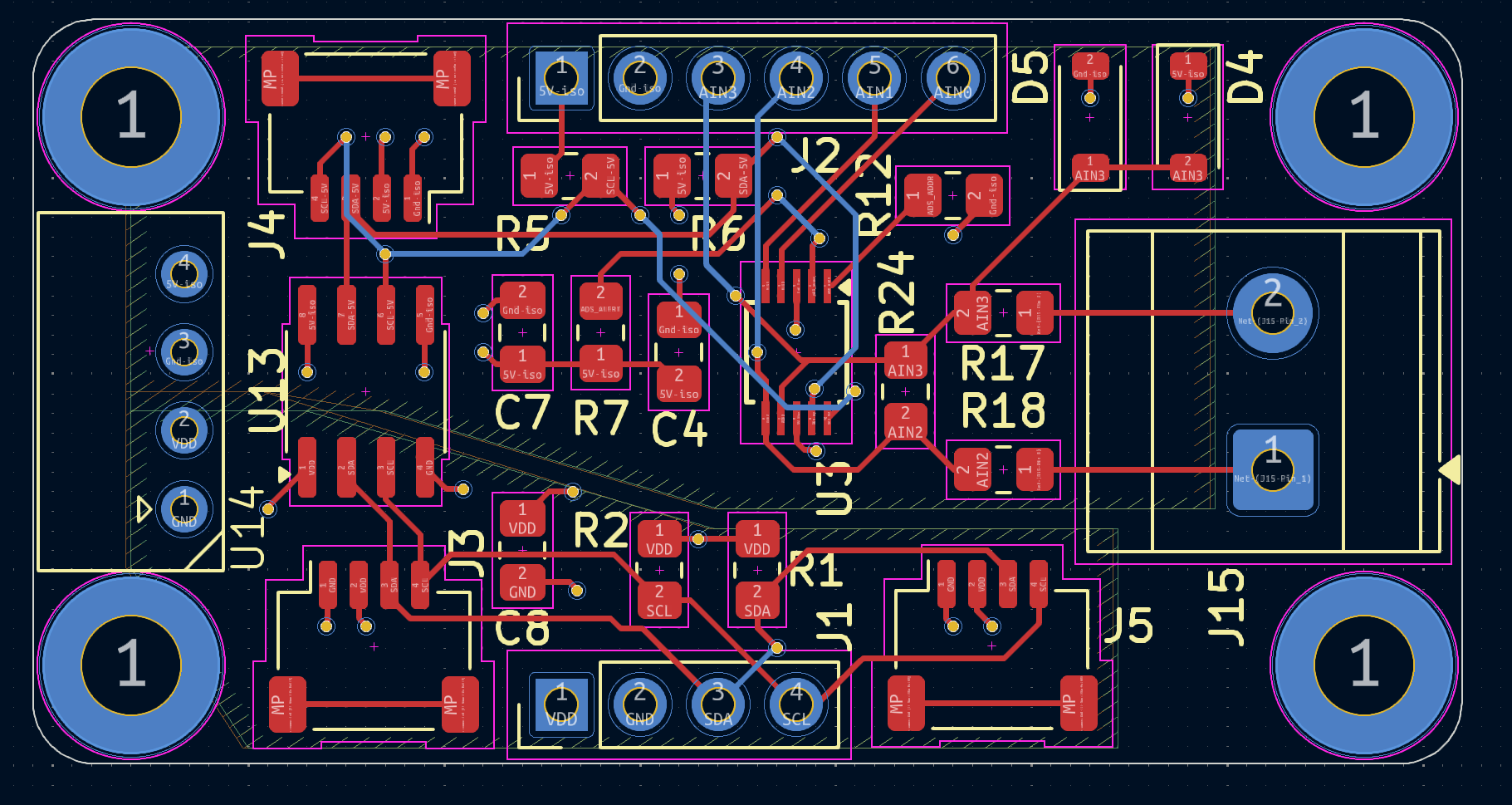
PCB View
Isolated Voltmeter Front End PCB
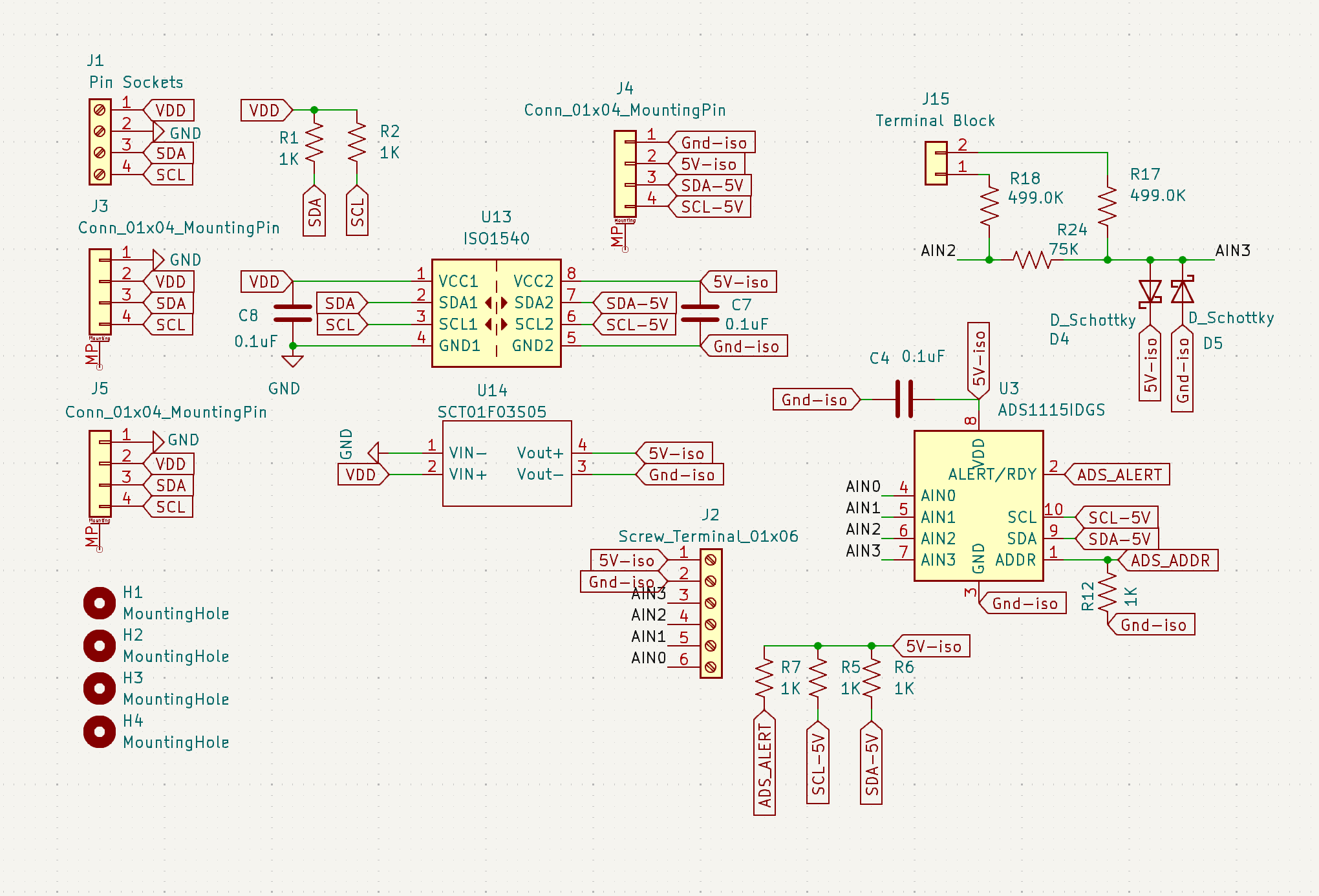
Schematic View
Function
This is an isolated voltmeter front end. The main components are an ADS1015 (ADC), ISO1540 (i2c bus isolator), and a SCT01F03S05 (3.3v to 5v isolated dc-dc converter). It additionally includes a voltage divider (with over-voltage protection) between the ADC 2-3 inputs. The board has jst-sh connections for the i2c bus (in addition to 0.1” pins) so it can be used with Stemma QT / Qwiic development boards.
Purpose
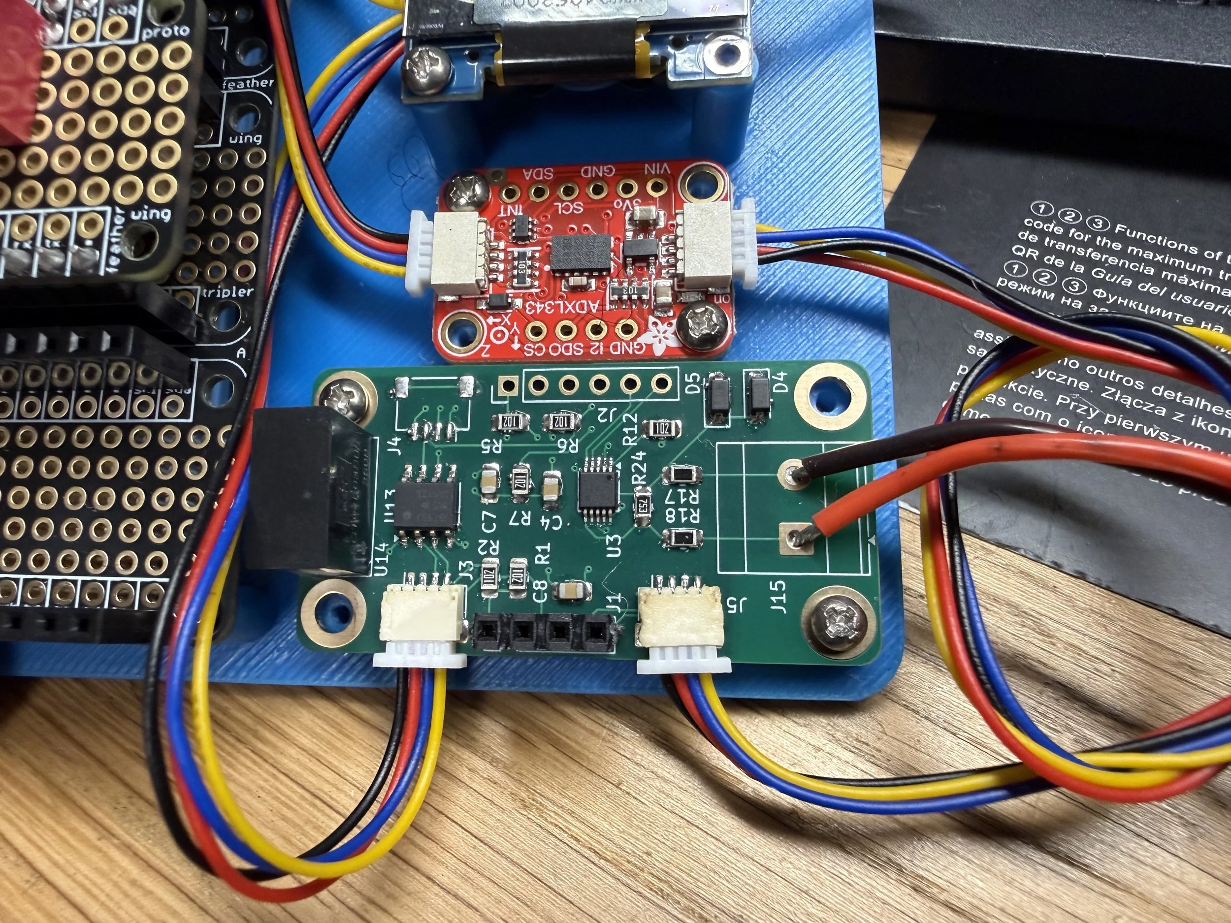
One of the assembled boards.
The purpose of this board is to allow voltage measurements isolated from the MCU’s ground reference. This prevents / mostly eliminates ground loops if e.g. the board is powered from the mains and you’re measuring something also powered from those same mains. The ADC can also measure arbitrarily low below ground in differential mode because it’s floating and therefore “sinks” to to match the lowest of the two input voltages. With a 1M/75K divider the input range is roughly +/-90V.
Note there are a pair of Schottky diodes to prevent overvoltage on the ADS inputs (although only for 2-3)
The isolation also allows shunt current measurements on high or low side.
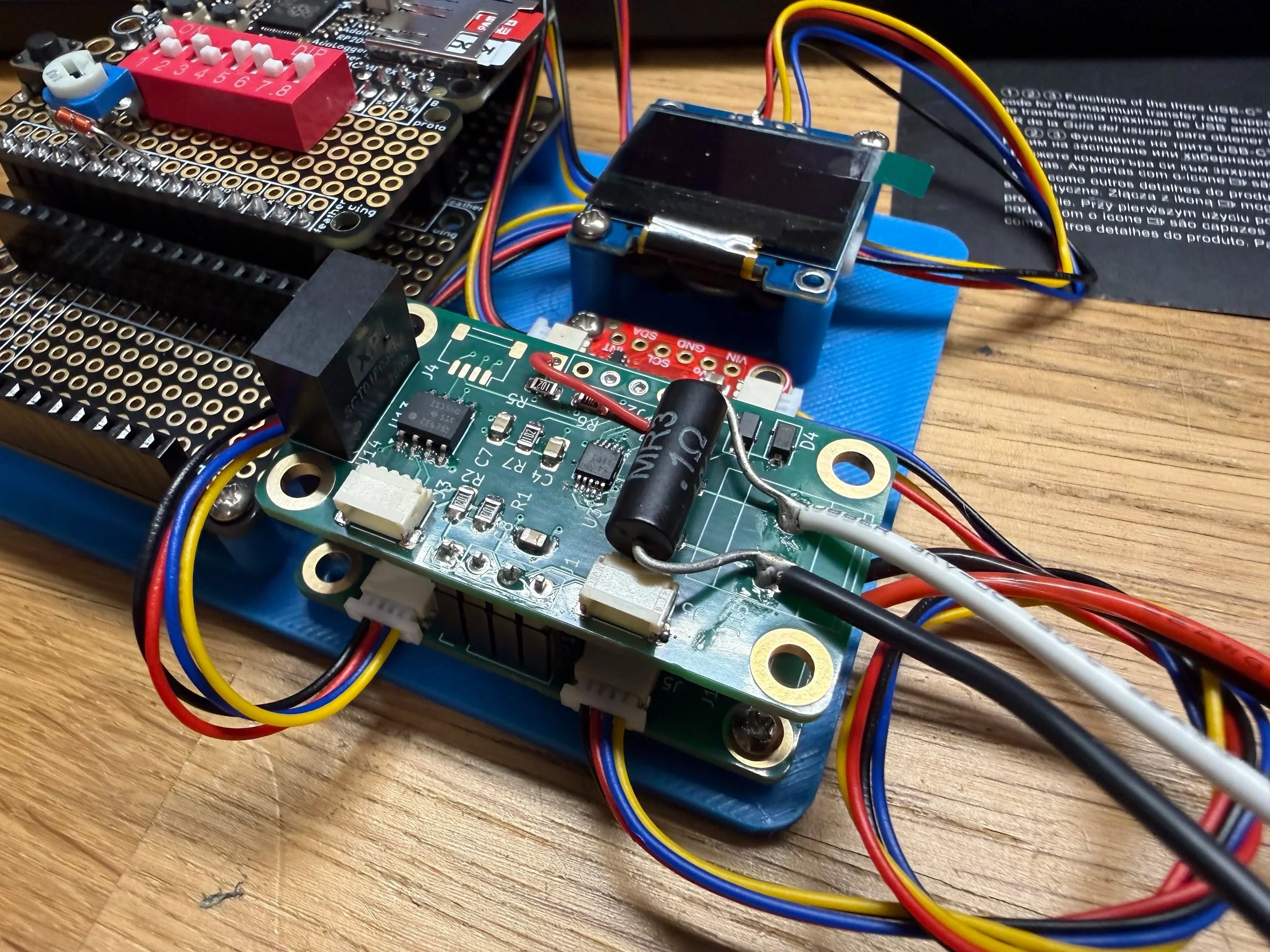
This PCB is modded for current measurement and a different i2c address and stacked on an non-modded board (with 0 Ohm jumpers for R17 and 18). This allows simultaneous isolated current and voltage measurements (so the current can be high side, low side, or a completely separate from the voltage).
Variations
Same PCB
The ADC can be either an ADS1015 or ADS1115 depending on more vs faster bits.
The DC-DC converter can be 5 to 5vdc instead of the 3.3 to 5vdc I have on their (standard i2c Stemma QT-style cable is 3.3v, so that’s the default config for this).
The voltage divider can be varied to whatever range someone desires.
The differential inputs can be screw terminals instead of wires.
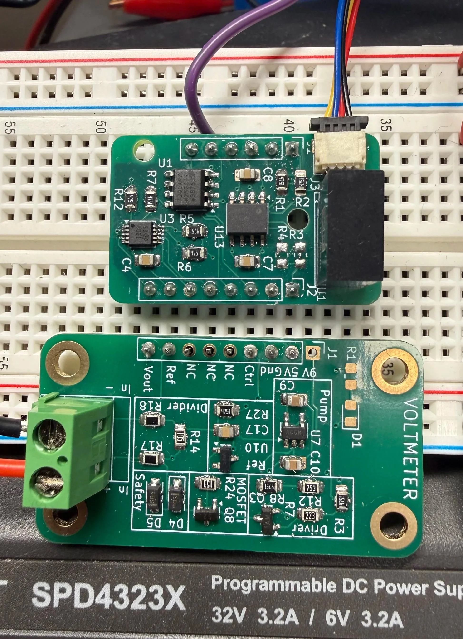
Isolated ADC board, top, and voltage conditioning + open lead detect, bottom.
Different PCB
I have another version of this board where I added an ADuM1200 chip for 2x binary signals across the isolation barrier (but no voltage conditioning, just the ADC input connections). This allows me to use my open-lead detect voltmeter circuits because that requires a MOSFET to turn on and off. I then have a voltage conditioning board with a matching pinout with the voltage condition and open-lead detect circuitry.
Cost
The board as pictured has a base cost of around ~$17 (early 2026). That’s $10 of components with $7 of PCB manufacturing (the PCBs themselves are closer to $3 each, with shipping and tariffs costing another $4).
Files:
In my GitHub, here: https://github.com/oihdesigns/Micro-DMM/tree/main/PCBDesigns/IsolatedADSBoard_V2
Want One?
I’m not in the business of selling these (at least right now), which is why I’m publishing the design files and otherwise making it easy for people to make their own. That said, if you want one I can also sell you one for $34 + shipping (*price subject to change). Email me for ordering details. I can also sell you just the PCB if you have your own components laying around.
Page info: First Published 26-1-18. This is the first version.