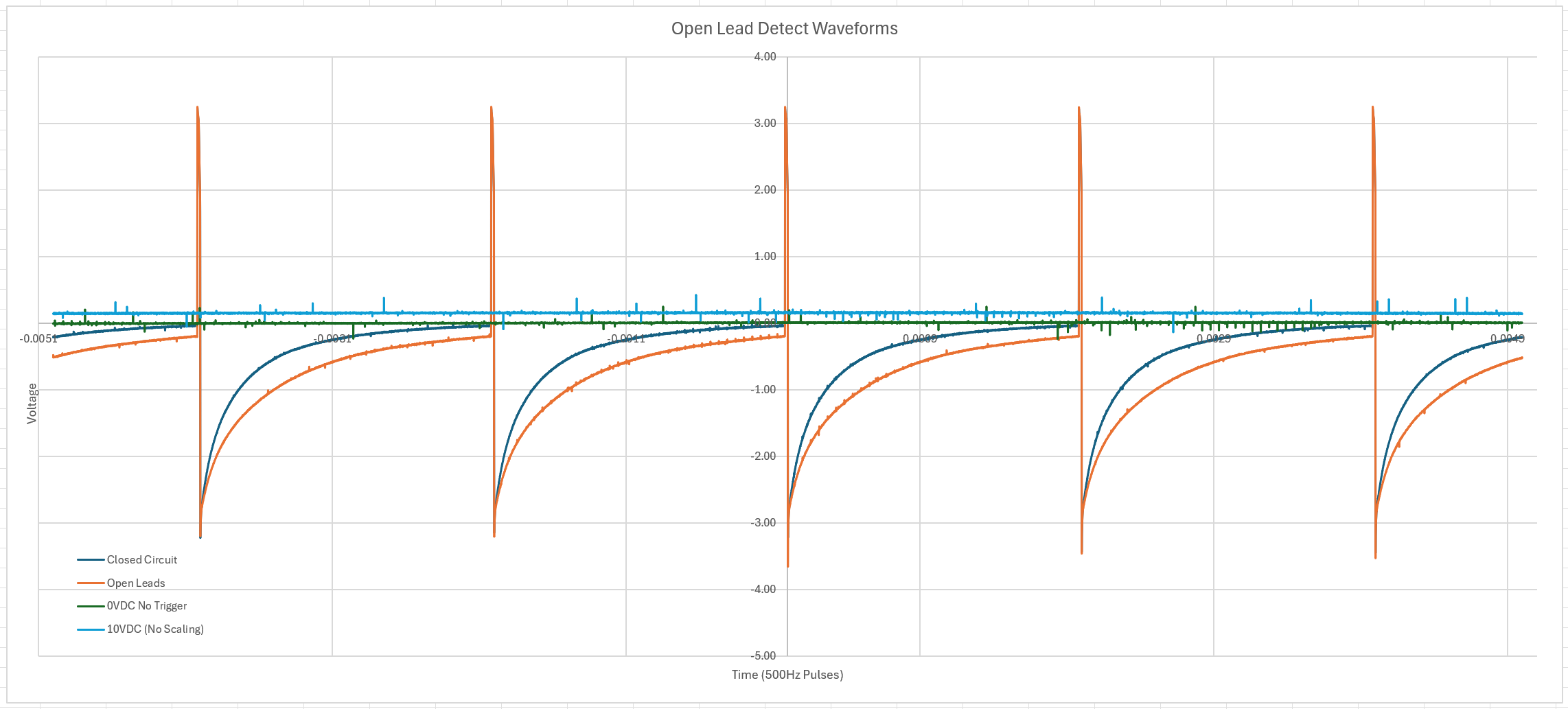
The Results from the Mann Voltmeter Bridge. The difference between the orange and deep blue curves indicate if a circuit is open or closed.
Voltmeter Open Lead Detect Circuit
As far as I can tell this is a novel voltmeter design, and as such I’m naming it the “Mann Voltmeter Bridge.” Am I right that this is novel? Given the best way to get the answer to something on the Internet is to post the wrong information, I’m assuming that someone will correct me if it’s not original (see contact page).
2026-3-15: Photos of the most recent iteration:
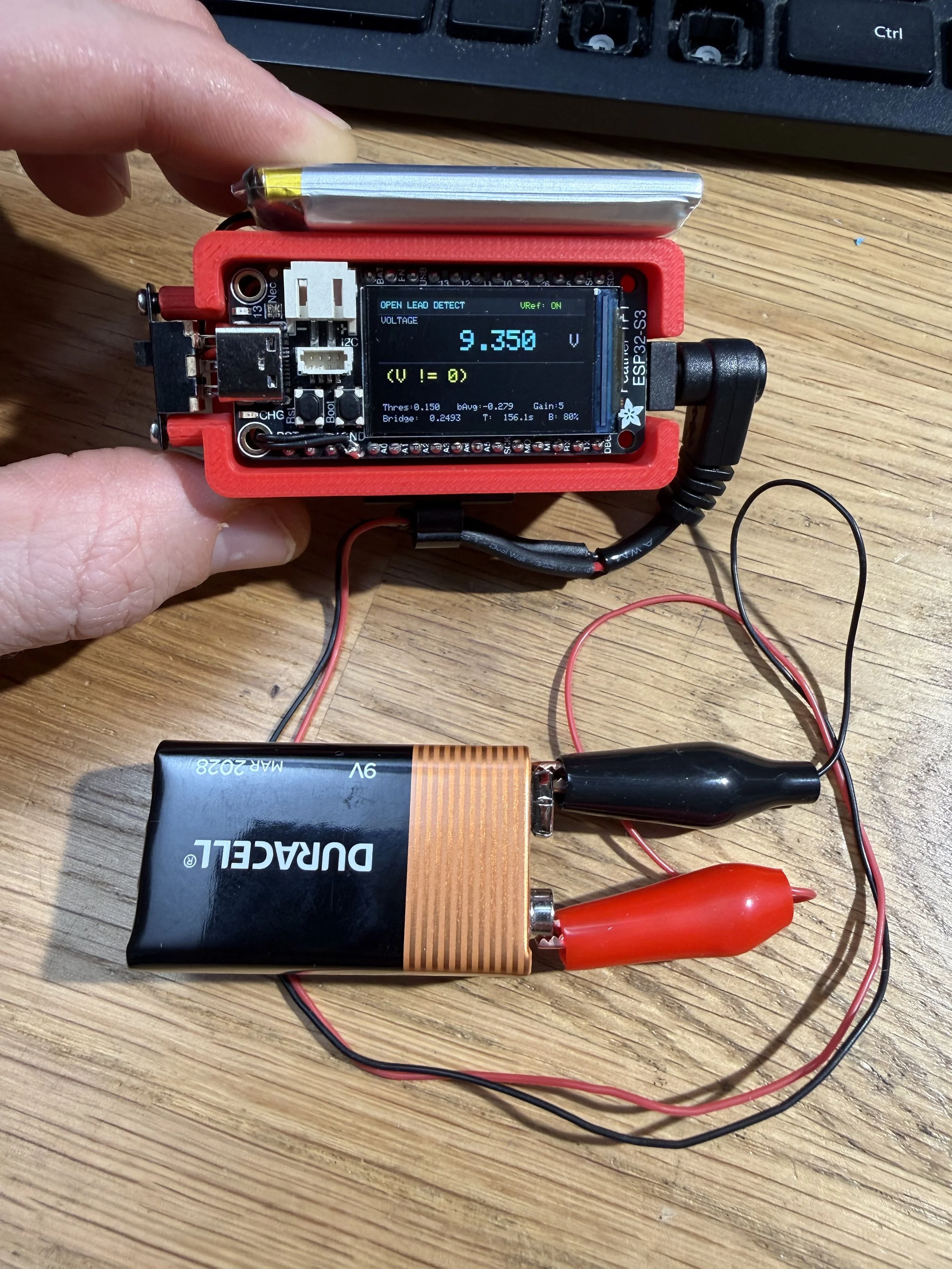
Reading Voltage
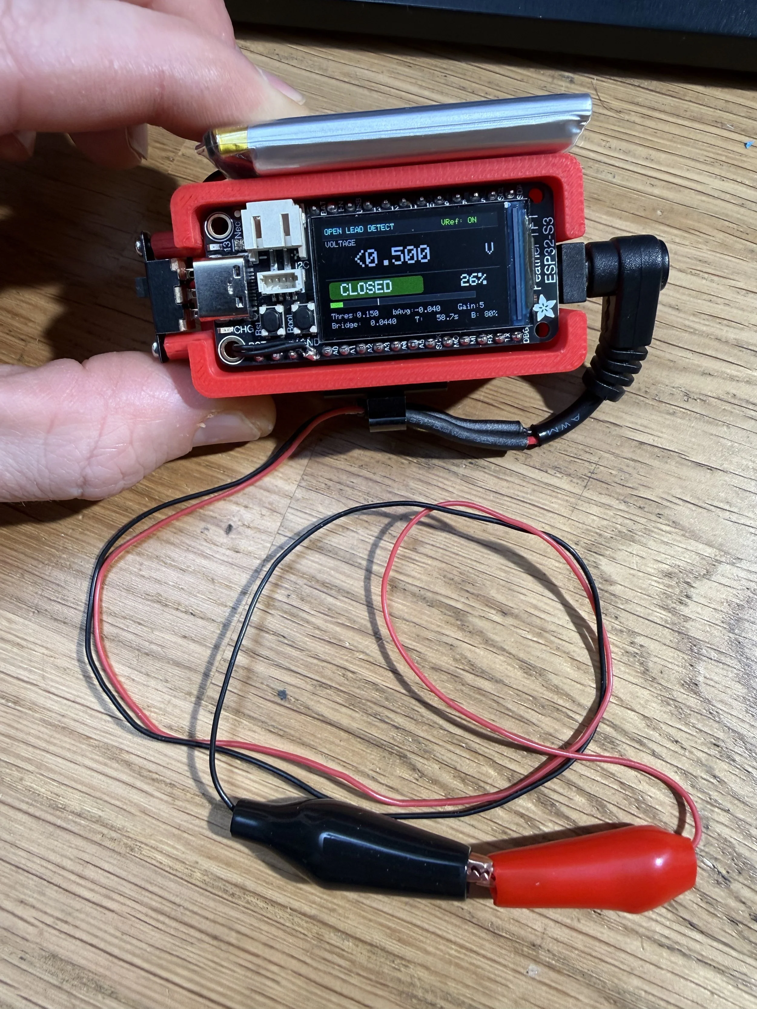
Indicating Closed
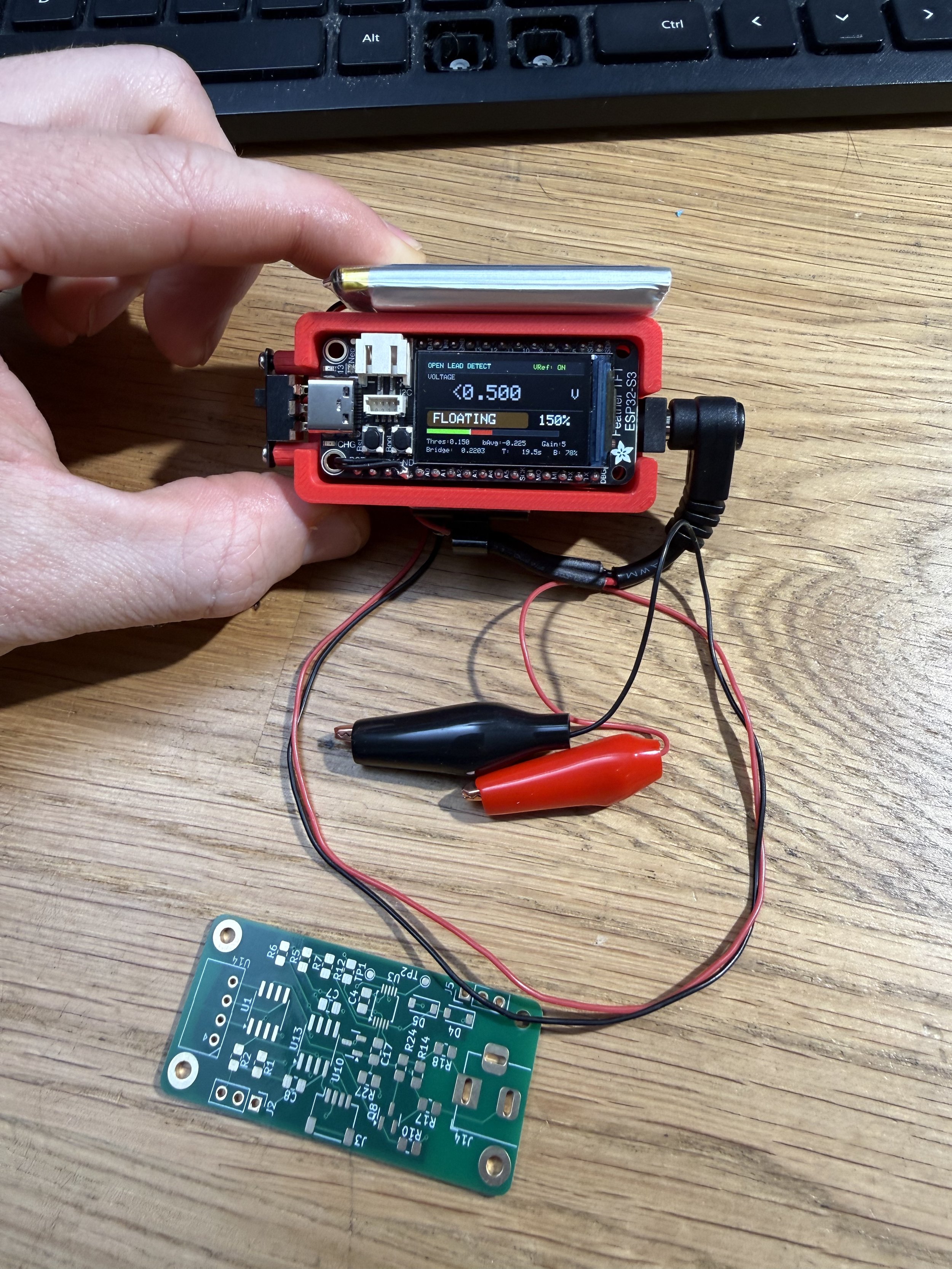
Indicating Floating
Above: This is a simplified proof-of-concept video showing just the circuit in use.
Below: These is a video where the circuit is integrated into my custom DMM.
Introducing the Mann Voltmeter Bridge Circuit. This is a voltmeter circuit that allows a voltmeter to distinguish when a zero volt reading means “floating probes” and when it means “the probes are on the same net.”
This was developed as part of my broader custom DMM / voltmeter project.
It works* by putting a MOSFET in a differential voltmeter bridge. Normally the MOSFET is closed, and it doesn’t affect voltmeter operation. When the ADC measures ~0v differential between sides the MOSFET is turned off, breaking the bridge and creating a transient, and the ADC measures the transient on the far side of the bridge. If the voltage is still about where is was before (2.5vdc in my circuit) that means the probes forming a closed circuit and the transient dissipated through the leads. If the ADC measures a different value (generally a dip below -300mV), that means the transient couldn’t go through the leads and lasted longer, indicating that the probes are floating.
*This is an approximation of the theory. I can confirm the circuit works, but some experimentation with variation inclines me to believe this can be even better characterized. It works, though.
This design allows the voltmeter to measure voltage (I’ve tested my circuit up to standard North American 120VAC) and automatically report to me voltage, open leads, or shorted leads on the fly.


Here is the circuit under different conditions (also see top image):

Measuring Voltage

Shorted Probes
I also have a second version of the bridge now, which adds a 1Meg resistor in parallel with both the MOSFET and the normal sense resistor. This resistor serves to both reduce the maximum voltage between the probe tips from ~2.5vdc to only 100mV, as well as further reduce the maximum possible current (down to 120nA).
The tradeoff with this circuit is that there is less information to tell you about impedance in an intermediate state (instead of 2v of signal to interpret you get 100mV). This is the alternate version (the new component is R9):

Characterizing the Behavior
Documenting the Functional Version
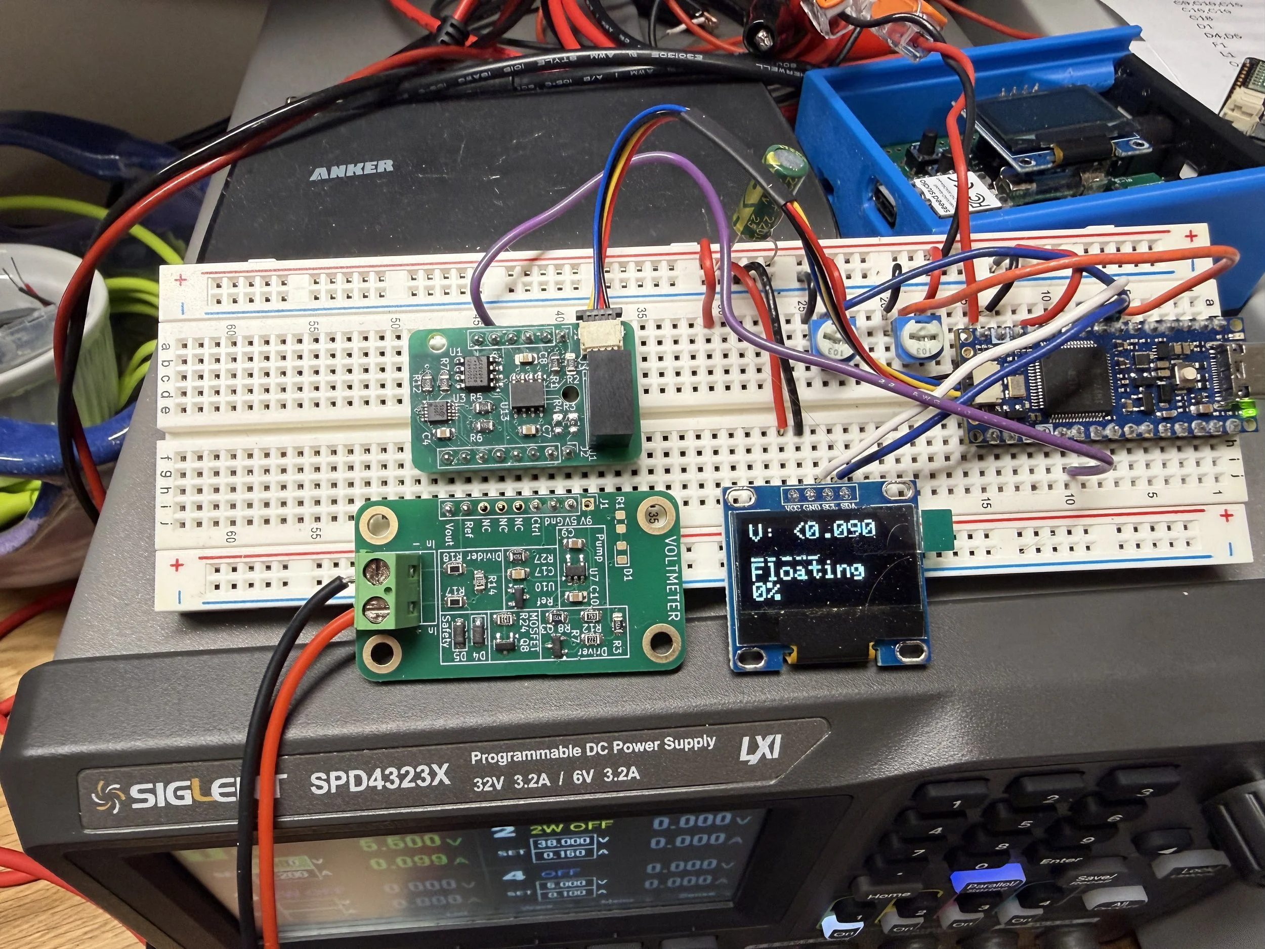
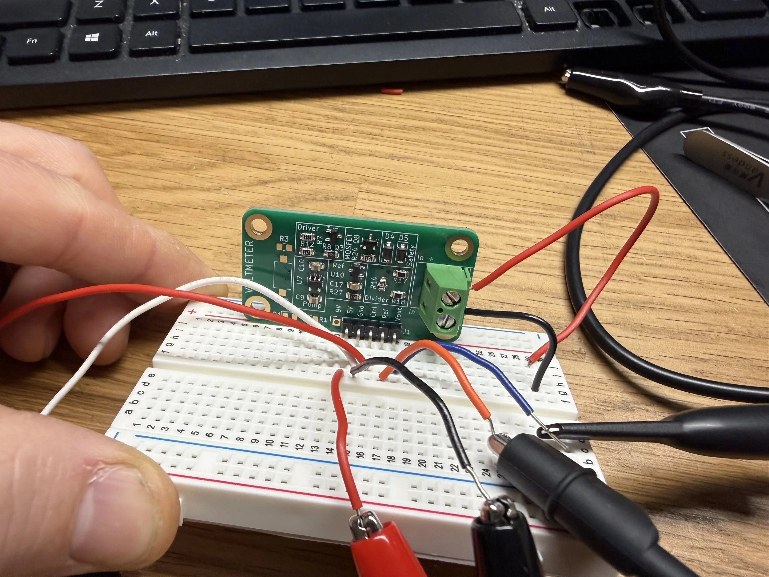
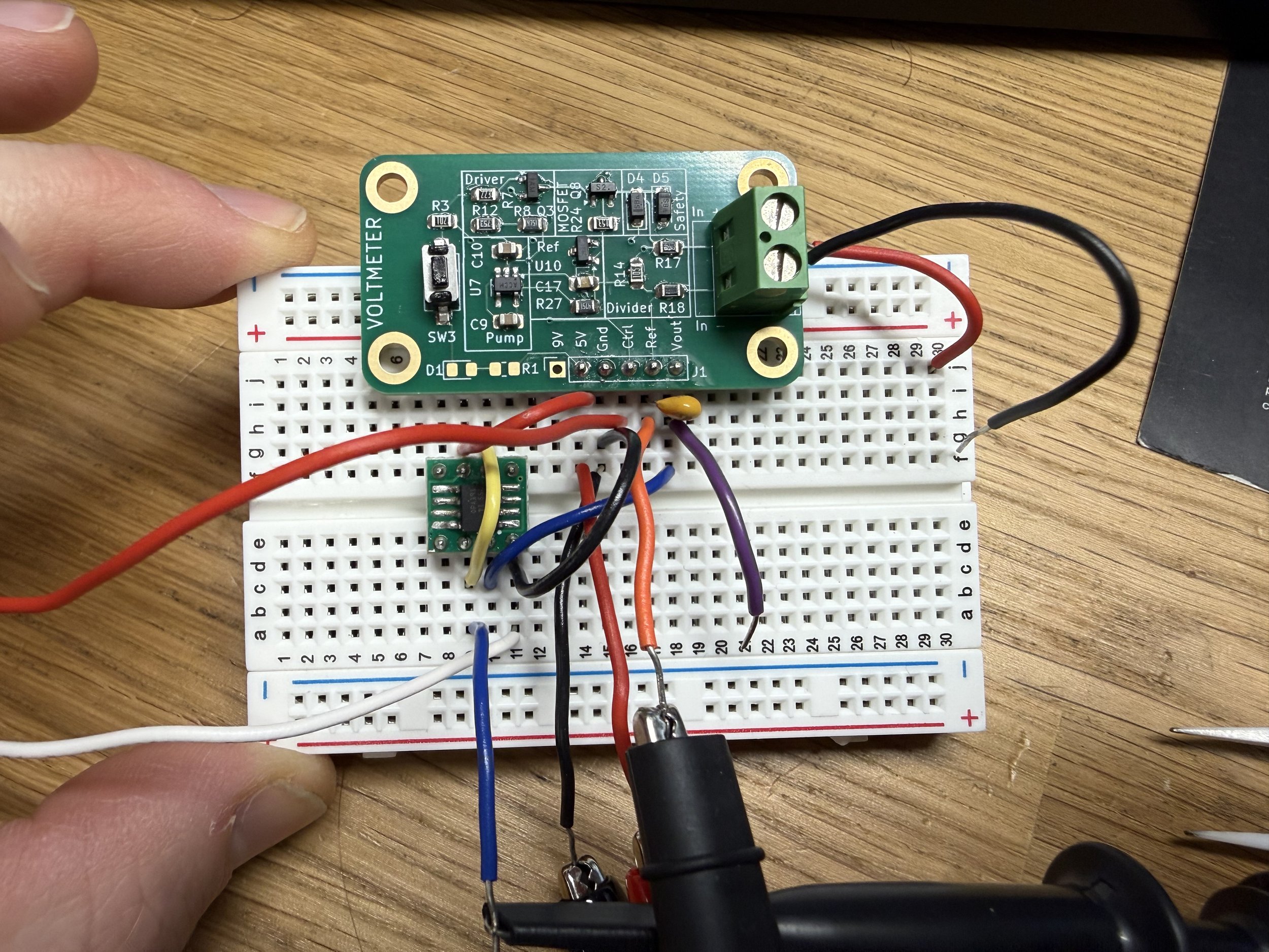
Below are the circuits I am using for this section (these are functionally the same as the setup in the “proof of concept” video at the top, but with dedicated PCBs instead of discreet modules/components):
*Note that I have made and tested this circuit with both an SI2302 an the AO3400 MOSFETs for Q8. The behavior is the same. The schematic below shows the AO3400, but these screenshots are technically of an SI2303 version.
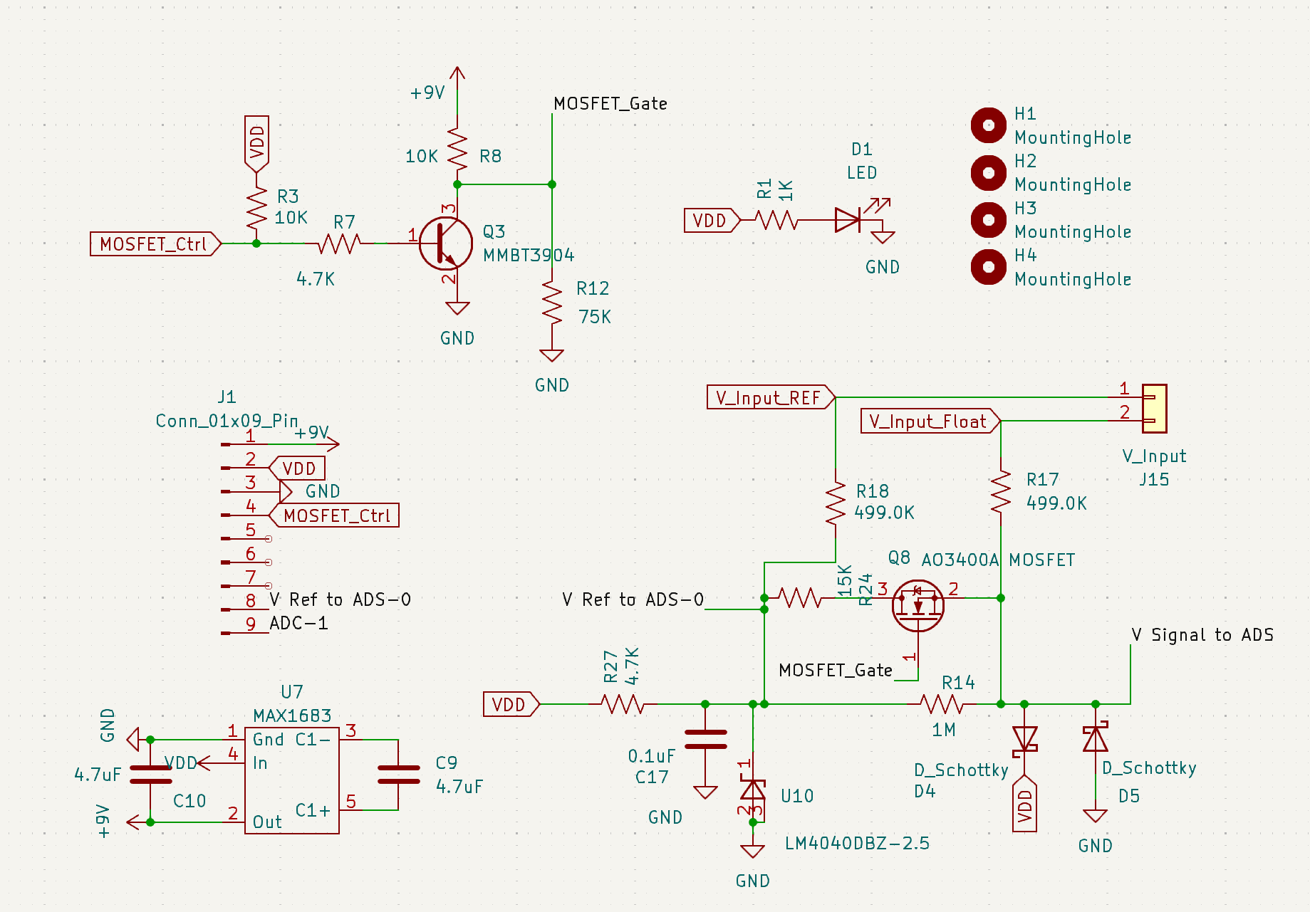
The Voltmeter Front End
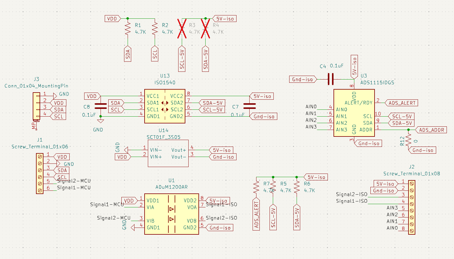
The Isolated ADC (ADS1115) and Signal (ADuM1200) Interface
Circuit I’m using.
Scope On Inputs
With this setup, when I attached a scope to the inputs I see this:
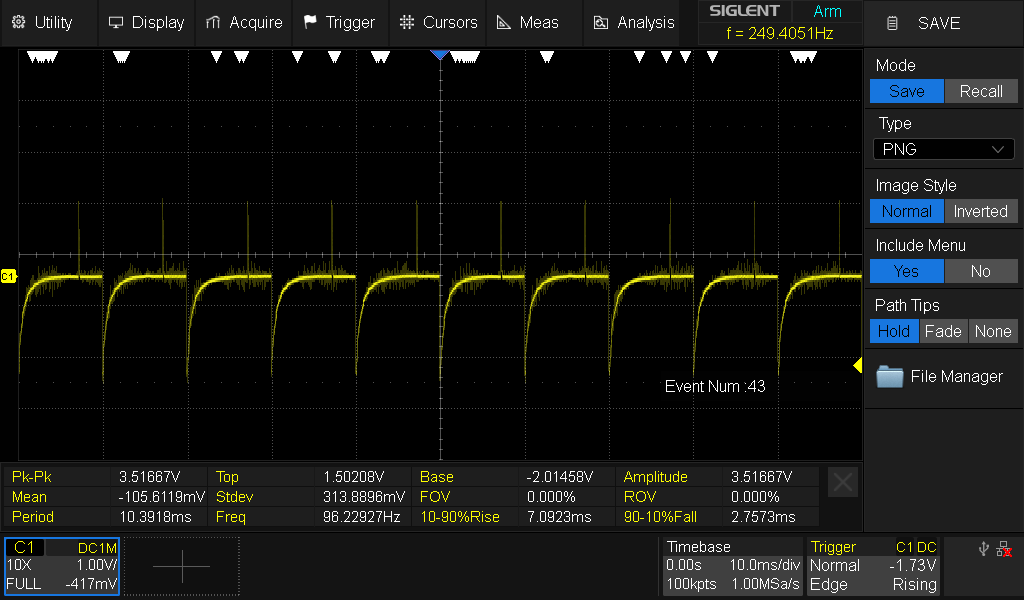
Screenshot of a scope. Note this is with the 10X on the probe.
Comparison at different input impedances (these are same scale / timebase):
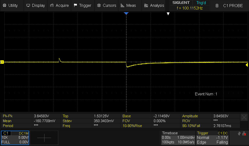
Here is a detail at 10X
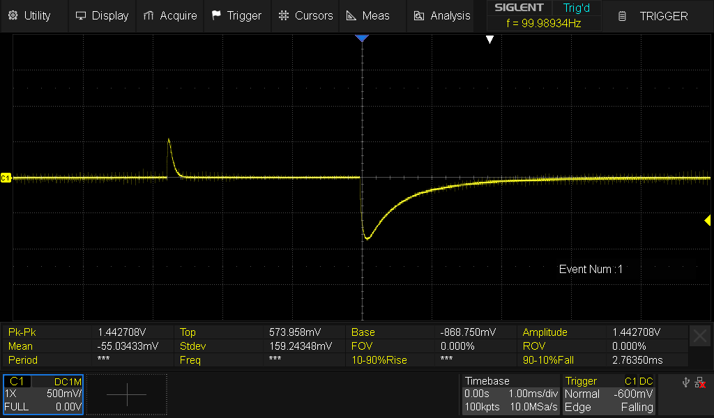
This is with the probe on 1X
The amplitude of that dip is the signal that allows the MCU to determine if the probes are open or closed (via a configurable threshold). As you can see, with the probe at 1X (1Meg) the dip is much smaller (~-0.8V) that with the higher (10Meg) impedance, where it’s about 2.1V.
Scope Reading Signal
Here I’m looking at just the voltmeter PCB. This abstracts away all the MCU and ADC components and gives me just the analog behavior. It is powered by a 5vdc supply and I have a function generator making a 5vdc 1% pulse at 500Hz to mimic the MCU controls. The probe is at 10x.
You can see the difference between open and closed circuits is the voltage falls back to zero faster in the closed circuit. (If I slow down the frequency the open lead curve falls to zero on it’s curve - it doesn’t level off first.)
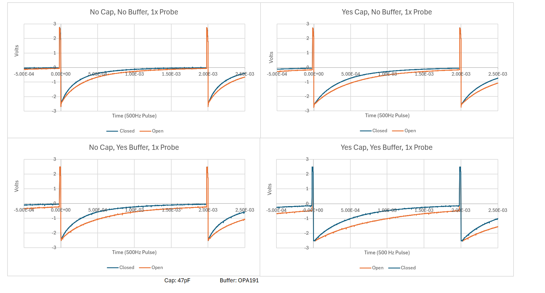
Buffering and Adding Capacitance to the Circuit:
Adding a capacitor and/or buffering the signal into the scope both improve signal strength. This is with the probe at 1x. Not 10x like above. The capacitor is across the analog output from the PCB.
Attempted Variations / Improvements [Under Construction]
I have attempted to make a version of this circuit where I could turn the voltage reference on and off. I wanted to completely remove the voltage reference from the circuit, so I used a photoMOS for the 2.5v (ref) rail. This broke the open lead detect for reasons I don’t particularly understand. I suspect my signal is dependent on the capacitor paired to the voltage reference, and this is an open area research.